
 Updated version of an article originally published in Personal Engineering and Instrumentation News,
September 1997, pages 53-56. (download
original in Adobat Acrobat format)
Updated version of an article originally published in Personal Engineering and Instrumentation News,
September 1997, pages 53-56. (download
original in Adobat Acrobat format)
One must consider many options when purchasing hardware and software for programmable-logic design. Choosing the right solution takes some time to evaluate various products. Some products demo well but come up short when you use them through the complete design process. Before embarking on a new design, one has to learn something about the tools involved. The methodology and software engineers use to complete a programmable-logic design are similar to those used for a board design. This article provides a basic overview of the design process and discusses the costs of associated hardware and software.
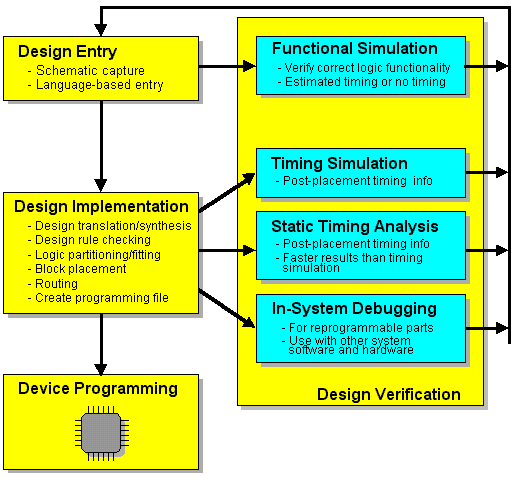
Programmable-logic design invariably involves four fundamental steps (see Figure 1):
Traditionally, schematic-based tools provided experienced designers with more control over the physical placement and partitioning of logic on a device. However, this extra tailoring takes time. Likewise, language-based tools allowed quick design entry but often at the cost of lower performance or density, although synthesis for language-based designs has significantly improved in the last few years, especially for FPGA design. In either case, learning the architecture and the tool help you create a better design. Technology-ignorant design is possible, but at the expense of density and performance.
To help speed development with
common design sections in any of
these environments, many chip vendors
provide intricate elements
known as cores. These specialized elements,
comprising such functionality
as a PCI-bus interface or a DMA
controller, are an increasingly important
addition to the programmable-logic
world. Core providers implement
and verify these predefined
functions in programmable-logic elements.
Cores have been available for
gate arrays for several years, but now
that FPGA devices push beyond the
50,000-gate density level, cores should
become a popular design-entry tool
for programmable logic, as well.
Physical implementation
After an engineer enters and synthesizes
a design (if using an HDL
instead of a schematic for entry), it’s
ready for implementation on the target
device. This first step involves
converting the design into a format
that the family-specific implementation
tools recognize. Most implementation
tools (also known as back-end
tools) read standard netlist formats,
and the translation process is usually
automatic.
Once the back-end tools translate an incoming netlist, they perform a design-rule check and optimize it. Then the software partitions designs into the logic blocks available on the device. Partitioning is an important step for both FPGAs and CPLDs because it results in higher-routing completion and better performance for FPGAs and increased density and performance for CPLDs.
Once it partitions a design into logic blocks, the implementation software searches for the best location to place each block among all of the possibilities. The primary goal is to reduce required routing resources and maximize system performance. This operation is compute intensive for FPGAs and larger CPLDs because the implementation software monitors routing length and track congestion while placing a large number of blocks. In some systems, the software also tracks path delays in order to meet user-specified timing constraints. Overall, the process mimics printed circuit-board placement and routing. After completing the place/route process, the software creates a binary programming file that configures the device, much like a board-layout package produces Gerber files at the end of its design flow.
In large or complex applications,
the software might not be able to place
and route the design. Some packages
try different options or run many iterations
in an attempt to obtain a fully
routed design. Generally, some designers
try to use less than 85% of
available device resources. This technique
gives the software extra resources
to help route a design. Also,
some vendors supply floorplanning
tools to aid in physical layout, which
is especially important for larger
FPGAs because some tools have problems
recognizing design structure. A
good floorplanning tool allows designers
to convey this structure to the
place/route software.
Design verification
Design verification exists at various
levels and steps throughout this
design process. Engineers should recognize
several fundamental types of
verification as applied to programmable
logic. Functional simulation
occurs in conjunction with design entry,
but before place and route, to
verify correct logic functionality,
while full-timing simulation must
wait until after the place/route step.
Then the software backannotates logic
and routing delays to the netlist for
simulation. While simulation is always
a good idea, programmable
logic usually doesn’t require the same
exhaustive timing stimulation that
gate arrays do.
In a gate array, full-timing simulation is important because the devices are mask-programmed and therefore not changeable. In addition, a design change typically involves thousands of extra dollars in non-recurring expenses (NRE) and weeks of time.
Compare this penalty to a programmable device where changes are possible in minutes to hours at little or no cost. With in-system programmable (ISP) devices, such as SRAM-based FPGAs and ISP CPLDs, changes are possible even while the parts are mounted in the system.
One successful and popular technique for programmable logic is to functionally simulate a design to guarantee proper logic execution, verify timing using a static timing calculator and then verify complete functionality by testing the design in the system.
Some device vendors supply additional
in-system debugging capabilities.
For example, Xilinx ships a
small pod called an XChecker cable
that connects to a PC’s serial port and
allows downloading of a design. With
a few simple additions to a design
and board, the XChecker cable can
stop or single-step the system clock
and read back the state of internal
flip-flops. Likewise, Actel’s Action
Probes provide access to internal
nodes within its antifuse based
FPGAs. However, keep one caveat in
mind--even though in-system de-bugging
is quick and relatively easy,
don’t view it as a complete replacement
for simulation.
Device programming
After creating and simulating a
programming file, you’re ready to
program the device. The method depends
on the target technology. Most
programmable-logic technologies, including
the PROMs used with SRAM-based
FPGAs, require some sort of a
device programmer. For a nominal
fee, a local distributor could perform
production programming, but you
generally need a low-volume device
programmer for development and
pre-production work.
In-system programmable devices, including SRAM-based FPGAs, might not require a physical programmer, but they do need some intelligent system resource to download the file into the device. In this case, a board design must account for this requirement by providing programming support with a microprocessor, microcontroller or a JTAG test port.
With design software you’ll find various options at $500 and below. Many vendors--including Actel, Lattice, Motorola, Philips and Xilinx--supply downloadable or free demo versions of their software for evaluation purposes. Most of these packages allow you to create complete designs for one or a few of their smaller devices (see the Resources list at the end of this column). At just below $500, Xilinx supplies complete schematic and simulation support for its lower-density FPGAs and all of its CPLD products. Altera offers a similar system, including logic synthesis, for under $1000.
Generally plan on spending $2500 to $20,000 for complete software, including logic-synthesis entry and broad support for a range of densities (all from one vendor, of course). Most programmable-logic suppliers don’t want the price of the development system to be an obstacle to a large-volume design. Additionally, most vendors provide the full software on a free evaluation basis for 30 days or more. Most also offer significant multiuser or site-license discounts. However, don’t forget the expense of software maintenance; most vendors charge roughly 15% of the purchase price per year for updates.
| Minimum Usable Machine | Recommended Machine |
|
|
Engineers purchasing a new machine for the job should realize they gain no benefit from an MMX-capable processor for PLD software. A dual-processor machine is beneficial, especially when working with bigger (about 20,000 gates and above) FPGA devices. The software, even under Windows NT, doesn’t execute any faster on a dual-processor machine, but the extra processor allows you to continue using the machine, while the other processor is consumed with placing and routing a large design. Be sure to buy enough memory to support the extra processor.
Larger devices, some now pushing past the 100,000-gate range, are massive memory hogs. If you plan on using these behemoths, be sure to stock up on enough RAM. Plan on a minimum of 64M bytes, with some vendors recommending 128M bytes or more. The bad news with memory requirements is that they’ll only get worse.
Another consideration is the operating system. Most vendors today support either Windows 95 or NT 4.0 or plan to do so in the immediate future. Anyone still using Windows 3.1 should plan on upgrading.
A modem and Internet connection are also no longer just nice to have. The various software and device vendors typically offer on-line technical support including software upgrades and the latest technical information. Some have just started releasing web-based software tools such as the Xilinx LogiCore PCI configuration tool. Also the Internet connection allows you to stay in contact with fellow engineers through newsgroups. One of the most relevant newsgroup to designers is COMP.ARCH.FPGA.
Antifuse-based devices usually require a more sophisticated programmer because the unit performs some device testing and antifuse integrity checking. Also, quad flat packages and other surface-mount components might need expensive sockets.
If you’re using SRAM-based FPGAs and plan to download the design from system memory to the FPGA with a processor or if you plan to have a system boot from an external byte-wide EPROM, an additional programmer might not be necessary-- a byte-wide EPROM programmer works fine. Likewise, if you’re using ISP or downloadable devices, again a programmer might not be necessary. The download cable should suffice for most prototyping.
 Copyright © 1997-98 by OptiMagic™, Inc. All rights reserved.