
 Updated version of an article originally published in Personal Engineering and Instrumentation News,
November 1997, pages 53-55. (download
original in Adobat Acrobat format)
Updated version of an article originally published in Personal Engineering and Instrumentation News,
November 1997, pages 53-55. (download
original in Adobat Acrobat format)
Many organizations promote an effective philosophy dubbed K.I.S.S. (for Keep It Simple, Stupid) to improve the success rate of complex operations. A variation of this theme promotes success in digital design: Keep It Strictly Synchronous.
The popularity and flexibility of array-based logic--whether a field-programmable gate array (FPGA), a complex programmable-logic device (CPLD) or a gate array--might tempt unwary designers into developing bad asynchronous habits. Because these devices all use programmable interconnect, different signal arrival times coupled with asynchronous logic invite a digital disaster.
Synchronous designs are inherently safer and easier to debug than asynchronous designs. Engineers can simply predict the behavior of synchronous systems and model them in simulation. The analysis comes down to the worst-case path between clock edges--a simple process, especially using a static timing analyzer. Asynchronous design involves analyzing all combinations of best- and worst-case signal paths over temperature, voltage and process--a far more onerous chore.
Consequently, synchronous designs work with a much wider variation in device timing parameters and over a broader temperature range than do most asynchronous designs. As process technology improves, circuit delays decrease. A vendor might ship faster devices that meet all datasheet specifications but behave differently than the old part. Problems with asynchronous logic usually don't appear until you've built a board. One batch of parts works fine, another batch fails the system test, while another batch seemingly fails intermittently in the field depending on operating conditions.
a.) Gated clock implementation fails
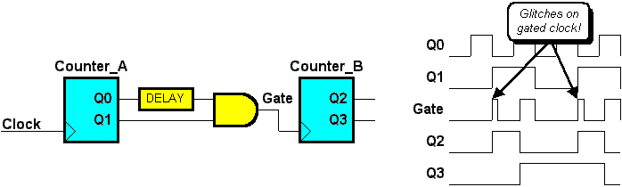
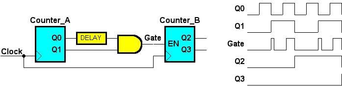
At first blush, you might think that you never use gated clocks. But all of the following situations involve a glitch-prone path through some combinatorial logic. For each circuit, there is an alternative, fully-synchronous implementation, usually involving a flip-flop with a Clock Enable input. In general, the clock for an internal flip-flop should only originate from either a device input or from another flip-flop. Consider these common situations:
architecture RTL of FlipFlop is
begin
   process (Reset, Clock)
   begin
      if (Reset = '1') then
         Output <= '0';
      elsif Clock'event and Clock = '1' then
         if (Enable = '1') then
            Output <= Data;
         end if;
      end if;
   end process;
end RTL;
|
always @ (posedge Clock or posedge Reset)
begin
   if (Reset)
      begin
         Output = 0;
      end
   else
      begin
         if (Enable)
            Output = Data;
      end
end
|
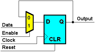
Figure 2. Some FPGAs have flip-flops with built-in clock enables, some don’t. Building an equivalent solution is simple as implemented in schematic (a), VHDL (b) and Verilog (c).
The solution in this example, and many others, includes a flip-flop with a Clock Enable input. In some FPGA devices, such as those from Xilinx and Lucent, the internal flip-flops have a built-in Clock Enable input. In other devices, you can easily build a clock input by including a 2:1 multiplexer in front of the data input (Figure 2). If designing circuits with VHDL or Verilog, note that not all synthesis packages automatically create a flip-flop using the built-in enable, even if one is available in the target technology.
A designer using CPLDs might wonder about the wisdom in using a product-term clock, which essentially is a gated clock. However, internal delays on a CPLD product term are more closely matched than routing delays inside an FPGA or gate array. However, you can still run into gated-clock problems on a product-term clock. Watch the inputs and their arrival times and be wary of potential glitches.
With most vendors’ tools, you must specifically request a global buffer either using a special symbol in the schematic or by instantiating the buffer through VHDL or Verilog, but some tools automatically infer the use of a global buffer. A downside of global clock buffers is that they’re among the largest power consumers in an FPGA or CPLD at somewhere between 2-10 mW/MHz. For most designs, this level is second only to I/O switching in overall power consumption. However, the benefit of a clock buffer typically outweighs the extra power consumption and engineering required to design without them. Luckily, in most devices you can connect as many flip-flops as desired to a buffer without consuming additional power. If a design requires the absolute minimum power and you decide not to use any global clock buffers, always be wary of clock-skew problems where the clock signal might arrive at one flip-flop before the others.
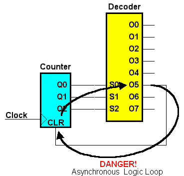
Many synchronous flip-flops, even with global clocks, use asynchronous Set and Reset inputs. Keep a watchful eye on these inputs. With modern fast devices, even a momentary glitch is enough to inadvertently change a flop’s state. Figure 3 shows a common circuit that decodes the output of a counter, and the decoded output asynchronously resets the counter. The problem is that a decoded output might be too short to reliably reset all the flip-flops in the counter. A better approach is to use a counter with a synchronous reset.
As mentioned for clock inputs, asynchronous flip-flop inputs should originate from either device inputs or from other flip-flop outputs.
 Copyright © 1997-99 by OptiMagic™, Inc. All rights reserved.