- Symbolic Address Name: MyRegister
The Symbolic Name is the name of the decoded address used in your program code. The actual address is assigned by the FastChip development system and communicated to your assembler/compiler via a generated header file.
- Decoded Read Signal Name: Read_MyReg
- Decoded Write Signal Name: Write_MyReg
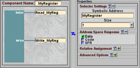
A Selector function from within the FastChip development system.
- Click the Selector function from the Triscend "soft" module library.
NOTE: Many other library functions include selector functions.
- Type in "Read_MyReg" in the RdSel text box. This assigns a signal called "Read_MyReg" to the Selector's RdSel output.
- Type in "Write_MyReg" in the WrSel text box.
- Type in "MyRegister" in the Symbolic Address text box. This assigns a symbolic address call "MyRegister" to this particular address.
- Set the size of the decoded address range using the Size droplist. The decoded range is always a power of 2, ranging from a single byte to 16 Mbytes.
- Indicate the types of instructions to which the Selector should respond using the check boxes
in the Address Space Response group. Multiple selections are allowed.
- Checking Data tells the Selector to respond to any data operations.
- Checking Code tells the Selector to respond to any code fetching operations.
- Checking SFR tells the Selector to respond as if it were one of the 8032's Special Function Registers (SFRs).
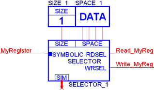
A Selector function defined using the OrCAD schematic editor.
- Select the Triscend library appropriate for your schematic editor.
- Choose the SELECTOR symbol from the library and place it on your schematic drawing.
- Assign the name of the decoded read signal by attaching a net to the "RDSEL" output. Name this signal "Read_MyReg".
- Assign the name of the decoded write signal by attaching a net to the "WRSEL" output. Name this signal "Write_MyReg".
- Assign the symbolic address name by attaching a net to the “SYMBOLIC” input. Name this signal "WriteRegister".
- Set the size of the decoded address space by attaching a "SIZE1" symbol to the "SIZE" port on the SELECTOR symbol. Various SIZE symbols are availabe to decode a range of address size, from a single byte (SIZE1) to 16 Mbytes (SIZE16M).
- Indicate which types of instructions to which the Selector should respond by attaching a “DATA” symbol to the "SPACE" port on the SELECTOR symbol. Separate symbols are available for each type.
- The "SIM" port is used for simulating bus transactions from within the schematic environment.