 Updated version of an article originally published in Personal Engineering and Instrumentation News,
July 1997, pages 75-78. (download
original in Adobat Acrobat format)
Updated version of an article originally published in Personal Engineering and Instrumentation News,
July 1997, pages 75-78. (download
original in Adobat Acrobat format)
If you’re not already using high-density programmable logic, it’s probably time to start. Prices for both devices and tools are dropping to where they’re attractive alternatives. In case you haven’t been watching, a massive battle is taking place for supremacy in the programmable-logic industry. The total market rocketed past the $1 billion mark as industry titans Xilinx, Altera, Actel, Lattice, Vantis and others fight for precious market share. As a result, device prices have dropped dramatically. A 2000-gate device that cost more than $100 in 1986 now sells for less than $5 in volume. Similarly, dramatic increases in density pushed gate counts well past the 50,000 mark.
Likewise, development software no longer costs between $5000 and $10,000. For $500 or less, a designer gets design-entry, implementation and simulation capabilities. Granted, a $500 package won’t provide all the options of a $5000 system, but it does provide sufficient capabilities for moderate-density designs. Further, broad support for programmable logic has emerged from CAE software companies. Even more importantly, high-end CAE suppliers now provide alternatives under Win95 and NT.
Thanks to these advances, programmable logic has become a mainstream technology. Look through electronics magazines, and you can’t miss ads for boards using it--even systems selling for less than $100. Another sign is that intellectual property (IP) companies now target their cores or hard macros for programmable logic as well as gate arrays. For engineering managers, it’s important to note that most recent EE graduates have gained experience with programmable logic as part of their undergraduate curriculum. Most recent graduates have the knowledge and skills to use these devices today.
Because the logic is on-site pro-grammable, design modifications and updates are far easier than with many other technologies. Most of a design resides on one or several chips, thereby reducing the number of "blue-wire" fixes tacked to the backside of a board. Also, changes cost little or nothing. At worst, you might throw away a few one-time programmable devices. Contrast this low cost of change to a gate array where modifications can cost $10,000 and weeks if not months of delay.
Further, many high-density devices are reprogrammable while in a system. Changes are practically free, and you can even make them when a board is deployed in the field. Some designers use this capability to adapt a board to unique configurations. Instead of shipping four different models for four applications, some companies ship one board that performs multiple tasks. This practice reduces engineering costs and simplifies manufacturing.
Design changes with programmable logic are also quick. An engineer can make a modification, recompile a design and download the change into the device in anywhere from 5 min to a few hours, depending on the device size and technology.
Obviously, programmable logic places other technologies. Because of its nature, designers use it in novel applications to replace or enhance existing processors. In some applications, especially DSP, specific compute- intensive algorithms consume most of a processor’s capability. Some designs implement these algorithms in hardware (with programmable logic) to offload time-critical or repetitive tasks. This specialized hardware frees the processor to perform other useful functions. For example, a 16-tap FIR filter in a field-programmable gate array (FPGA) can outperform a standard DSP chip by a factor of ten or more. In another example, a board full of FPGAs outperformed a Cray supercomputer in a pattern-matching application for the Human Genome Project. Programmable logic is also an enabling technology for a new field called reconfigurable computing in which a designer tailors the processing element to the specific application. This customization provides significantly higher performance than is possible with standard processors.
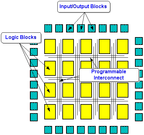
This group breaks down into a wide variety of subarchitectures, but you’ll find two primary classes of FPGA architectures. First, coarse-grained architectures consist of fairly large logic blocks, often containing two or more lookup tables and two or more flip-flops. In these architectures, a 4-input lookup table (think of it as a 16 x 1 ROM) implements the actual logic.
The other architecture is called fine-grained. These devices hold a large number of relatively simple logic blocks. Each block usually contains a flip-flop and either a 2-input logic function or a 4:1 multiplexer. These devices excel at bit-serial functions such as shift registers, corner benders or serial arithmetic, and they offer benefits for logic-synthesis-generated designs.
Another difference in architectures concerns the underlying process technology. Currently, the highest-density FPGAs use static memory (SRAM) technology, similar to micro-processors. The other common process technology is antifuse, which has benefits for programmable interconnect (see Table 1).
| Architecture | Static Memory | Anti-Fuse | Flash |
| Coarse-grained | Altera: (FLEX) Atmel: (AT40K) DynaChip Lucent: (ORCA) Vantis: (VF1) Xilinx: (XC3000,XC4000xx,Spartan,XC5200) |
QuickLogic | . |
| Fine-grained | Actel: (SPGA) Atmel: (AT6000) Motorola Xilinx: (XC6200) |
Actel: (ACT) | Gatefield |
NOTE: Also see the summary table of programmable devices and manufacturers.
SRAM-based devices are inherently reprogrammable, even in-system. A configuration memory holds the program that defines how each logic block functions, whether I/O blocks serve as inputs and outputs and how blocks connect to each other. An FPGA either self-loads its configuration program, or an external processor downloads the program. When self-loading, an FPGA addresses a standard byte-wide memory much like a processor or uses a special sequential-access serial PROM. When a processor downloads a program, an FPGA appears much like a standard microprocessor peripheral. The configuration time is typically < 200 msec, depending on device size and configuration method.
In contrast, antifuse devices are one-time programmable (OTP). Once programmed, they can’t be modified but do retain their program when power is off. Antifuse devices require a specialized or a high-end programmer, as most programmers don’t support antifuse.
Many course-grained FPGAs also contain system-level features to boost performance or to simplify system design. For instance, dedicated carry logic boosts performance for arithmetic functions and counters. Bidirectional busing mirrors what you’ll find on many boards and systems, allowing easy integration of bused registers and other logic elements. Further, on-chip RAM simplifies register files, FIFOs and small data-buffering applications.
Generally, FPGAs have many more
registers and I/O than CPLDs and
typically use less power. FPGAs are
usually best for datapath-oriented
design but don’t have the fast pin-to-pin
performance associated with
CPLDs.
CPLD (Complex Programmable
Logic Device)
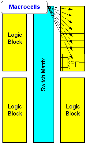
In concept, CPLDs consist of multiple
PAL-like logic blocks interconnected
with a programmable switch
matrix (Fig 2). Typically, each logic
block contains four to 16 macrocells
depending on the vendor and the
architecture.
A macrocell on most modern CPLDs contains a sum-of-products combinatorial logic function and an optional flip-flop. The combinatorial logic function typically supports four to 16 product terms with wide fan-in. In other words, a macrocell function can have many inputs, but the complexity of the logic function is limited. Contrast this structure to an FPGA logic block where complexity is unlimited, but the lookup table has only four inputs.
CPLDs provide a natural migration path for PAL designers seeking higher density. They offer a PAL-like architecture, and generally four or more PALs comfortably fit into a CPLD. Most CPLDs support PAL development languages such as ABEL, CuPL and Palasm.
CPLDs are generally best for control- oriented designs due in part to their fast pin-to-pin performance. The wide fan-in of their macrocells makes them well-suited to complex, high-performance state machines.
One major variation among CPLD architectures concerns how they deal with insufficient product terms. In some architectures, when the number of product terms a design requires exceeds the number available in the macrocell, design software borrows terms from an adjoining macrocell. When borrowing terms, the adjoining macrocell might not be useful any longer in some architectures, while in others, the macrocell retains some basic functionality. In addition, bor-rowed product terms usually increase propagation delay.
Another difference deals with the number of connections within the switch matrix. A switch matrix supporting all possible connections is fully populated, while a partially populated switch supports most connections. The number of connections within the matrix determines how easily a design fits in a given device. With a fully populated switch matrix, a design routes even with a majority of the device resources used and with fixed I/O pin assignment. Generally, delays within a fully populated switch matrix are fixed and predictable.
A device with a partially populated switch matrix might present problems to tools when routing complex designs. Also, it might be difficult to make design changes in these devices without altering the pinout. Routing to a fixed pinout is important because it’s easier to change the internals of a PLD than to relay out a circuit board. Though a partially populated switch matrix is less expensive to manufacture, it might be more difficult to use. The delays within a partially populated matrix can’t be fixed and aren’t easy to predict.
CPLDs are based on one of three process technologies
EEPROM and FLASH processes are erasable technologies. However, not all EEPROM- and FLASH-based devices are programmable while soldered on a board. In-system programmability (ISP) requires special on-chip programming logic, and not all CPLDs come with it, even when built with EEPROM and FLASH technologies. You can erase and program those lacking that circuitry in a device programmer. Those with the circuitry either use a vendor-proprietary interface or a JTAG (IEEE 1149.1) interface for programming.
http://www.reconfig.com/gloss.htm.
 Copyright © 1997-98 by OptiMagic™, Inc. All rights reserved.