
The following is a list of frequently-asked questions about programmable logic technologies including FPGAs, CPLDs, FPICs, and their associated design tools. The Programmable Logic FAQ was written and is maintained by Steve Knapp, a former application engineer for Xilinx, Inc. and Intel's programmable logic division, purchased by Altera a few years ago.
| I M P O R T A N T !
This page is a work in progress and is subject to frequent updates. Please note that this is copyrighted material and cannot be reproduced without the prior written permission of OptiMagic, Inc. |
What is programmable logic?What kinds of programmable logic devices are available today? How are they different from one another?
How do I design with programmable logic?
Which companies supply programmable logic?
I would like to try programmable logic but I don't want to spend a lot of money just yet. Where can I get inexpensive design tools?
I currently design with gate arrays or ASICs. What are the advantages and disadvantages of using programmable logic?
What does 'in-circuit programmable' or 'in-system programmable (ISP)' mean?
What general advice can you give to a programmable logic user?
What is programmable logic?
Programmable logic is loosely defined as a device with configurable logic and flip-flops linked together with programmable interconnect. Memory cells control and define the function that the logic performs and how the various logic functions are interconnected. Though various devices use different architectures, all are based on this fundamental idea.
What kinds of programmable logic devices are available today? How are they different from one another?
There are a few major programmable logic architecture available today. Each architecture typically has vendor-specific sub-variants within each type. The major types include:
- Simple Programmable Logic Devices (SPLDs),
- Complex Programmable Logic Devices (CPLDs), and
- Field Programmable Gate Arrays (FPGAs)
- Field Programmable InterConnect (FPICs)
SPLD - Simple Programmable Logic Device
Also known as:SPLDs are the smallest and consequently the least-expensive form of programmable logic. An SPLD is typically comprised of four to 22 macrocells and can typically replace a few 7400-series TTL devices. Each of the macrocells is typically fully connected to the others in the device. Most SPLDs use either fuses or non-volatile memory cells such as EPROM, EEPROM, or FLASH to define the functionality.
- PAL (Programmable Array Logic, Vantis)
- GAL (Generic Array Logic, Lattice)
- PLA (Programmable Logic Array)
- PLD (Programmable Logic Device)
CPLD - Complex Programmable Logic Device
Also known as:CPLDs are similar to SPLDs except that they are significantly higher capacity. A typical CPLD is the equivalent of two to 64 SPLDs. A CPLD typically contains from tens to a few hundred macrocells. A group of eight to 16 macrocells is typically grouped together into a larger function block. The macrocells within a function block are usually fully connected. If a device contains multiple function blocks, then the function blocks are further interconnected. Not all CPLDs are fully connected between function blocks-this is vendor and family specific. Less that 100% connection between function blocks means that there is a chance that the device will not route or may have problems keeping the same pinout between design revisions.
- EPLD (Erasable Programmable Logic Device)
- PEEL
- EEPLD (Electrically-Erasable Programmable Logic Device)
- MAX (Multiple Array matriX, Altera)
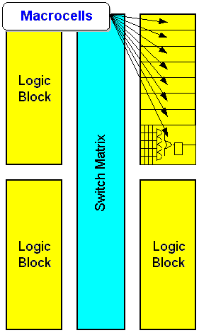
In concept, CPLDs consist of multiple PAL-like logic blocks interconnected together via a programmable switch matrix. Typically, each logic block contains 4 to 16 macrocells, depending on the architecture.
CPLDs provide a natural migration path for SPLD designers seeking higher density. CPLDs have a PAL-like architecture and generally four or more PALs comfortably fit into a CPLD. Most CPLDs support the SPLD development languages such as ABEL, CuPL, PALASM, etc.
CPLDs are generally best for control-oriented designs, due in part to their fast pin-to-pin performance. The wide fan-in of their macrocells makes them well-suited to complex, high performance state machines.
Some of the major variations between CPLD architectures include the number of product terms per macrocell, whether product terms from one macrocell can be borrowed or allocated to another macrocell, and whether the interconnect switch matrix is fully- or partially-populated.
In some architectures, when the number of product terms required exceeds the number available in the macrocell, additional product terms are borrowed from an adjoining macrocell. This makes the CPLD device useful for a wider variety of applications. When borrowing product terms from an adjoining macrocell, that macrocell may no longer be useful. In some architectures, the macrocell still has some basic functionality. Borrowed product terms usually means increased propagation delay.
Another difference in architectures is the number of connections within the switch matrix. A switch matrix supporting all possible connections is fully populated. A partially- populated switch supports most, but not all, connections. The number of connections within the switch matrix determines how easy a design will fit in a given device. With a fully-populated switch matrix, a design will route even with a majority of the device resources used and with fixed I/O pin assignment. Generally, the delays within a fully populated switch matrix are fixed and predictable.
A device with a partially-populated switch matrix may have problems routing complex designs. Also, it may be difficult to make design changes in these devices without using a different pinout. Routing to a fixed pinout is important. It is far easier to change the internals of a programmable logic device than it is to re-layout a circuit board. The delays within a partially-populated switch matrix are not fixed and less easily predicted, similar to most FPGA devices. Though a partially populated switch matrix has some potential limitations, it is less expensive to manufacture.
CPLDs are manufactured using one of three process technologies-EPROM, EEPROM, or FLASH. EPROM-based CPLDs are usually one-time programmable (OTP) unless they are in an UV-erasable windowed package. A device programmer or the manufacturer or distributor programs an EPROM-based CPLD.
Generally, CPLDs are CMOS and use non-volatile memory cells such as EPROM, EEPROM, or FLASH to define the functionality. Many of the most-recently introduced CPLD families use a EEPROM or FLASH and have been designed so that they can be programmed in-circuit (also called ISP for in-system programmable).
Table 1. CPLD Devices and Programming. Programmer Required In-Circuit Programmable Altera
Atmel
Cypress
Lattice
Philips
Vantis
XilinxAltera
Cypress
Lattice
Vantis
Xilinx
FPGA - Field Programmable Gate Array
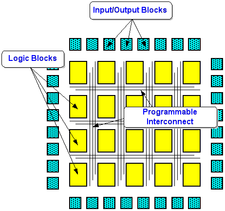
Also known as:FPGAs are a distinct from SPLDs and CPLDs and typically offer the highest logic capacity. An FPGA consists of an array of logic blocks, surrounded by programmable I/O blocks, and connected with programmable interconnect. A typical FPGA contains from 64 to tens of thousands of logic blocks and an even greater number of flip-flops. Most FPGAs do not provide 100% interconnect between logic blocks (to do so would be prohibitively expensive). Instead, sophisticated software places and routes the logic on the device much like a PCB autorouter would place and route components.
- LCA (Logic Cell Array)
- pASIC (programmable ASIC)
- FLEX, APEX (Altera)
- ACT (Actel)
- ORCA (Lucent)
- Virtex (Xilinx)
- pASIC (QuickLogic)
A generic description of an FPGA is a programmable device with an internal array of logic blocks, surrounded by a ring of programmable input/output blocks, connected together via programmable interconnect. There are a wide variety of sub-architectures within this group. The secret to density and performance in these devices lies in the logic contained in their logic blocks and on the performance and efficiency of their routing architecture.
There are two primary classes of FPGA architectures:
Coarse-grained architectures consist of fairly large logic blocks, often containing two or more look-up tables and two or more flip-flops. In a majority of these architectures, a four-input look-up table (think of it as a 16x1 ROM) implements the actual logic. The larger logic block usually corresponds to improved performance.
- coarse-grained, and
- fine-grained.
Table 1. FPGA Architectures and Processes. Architecture Static Memory Anti-Fuse Flash Coarse-grained Altera: (FLEX, APEX)
Atmel: (AT40K)
DynaChip
Lucent: (ORCA)
Vantis: (VF1)
Xilinx: (XC3000,XC4000xx,Spartan,Virtex)QuickLogic: (pASIC) . Fine-grained Actel: (SPGA)
Atmel: (AT6000)
Actel: (ACT) Gatefield NOTE: Also see the summary table of programmable devices and manufacturers.
The other architecture type is called fine-grained. In these devices, there are a large number of relatively simple logic blocks. The logic block usually contains either a two-input logic function or a 4-to-1 multiplexer and a flip-flop. These devices are good at systolic functions and have some benefits for designs created by logic synthesis.
Another difference in architectures is the underlying process technology used to manufacture the device. Currently, the highest-density FPGAs are built using static memory (SRAM) technology, similar to microprocessors. The other common process technology is called anti-fuse, which has benefits for more plentiful programmable interconnect.
SRAM-based devices are inherently re-programmable, even in-system. However, they require some form of external configuration memory source. The configuration memory holds the program that defines how each of the logic blocks functions, which I/O blocks are inputs and outputs, and how the blocks are interconnected together. The FPGA either self-loads its configuration memory or an external processor downloads the memory into the FPGA. When self-loading, the FPGA addresses a standard byte-wide PROM-much like a processor addresses its boot PROM-or uses a special sequential-access serial PROM. When downloaded by a processor, the FPGA appears much like a standard microprocessor peripheral. The configuration time is typically less than 200 ms, depending on the device size and configuration method.
In contrast, anti-fuse devices are one-time programmable (OTP). One programmed, they cannot be modified, but they also retain their program when the power is off. Anti-fuse devices are programmed in a device programmer either by the end user or by the factory or distributor.
Some FPGAs have system-level features built-in like on-chip bussing, on-chip RAM for building small register files or FIFOs, and built-in JTAG boundary-scan support.
Most FPGAs use either SRAM or anti-fuse CMOS technology. SRAM-based FPGAs are in-system programmable whereas anti-fuse-based FPGAs are one-time programmable.
FPIC - Field Programmable Interconnect Device
An FPIC is not really a logic device but rather a programmable "wiring" device. Through programming, an FPIC connects one pin on the device to another on the device providing programmable interconnect. FPICs use either SRAM or anti-fuse programming technology.I-Cube provides FPIC devices as stand-alone components. Aptix sells their FPIC devices as part of their hardware emulation system.
How do I design with programmable logic?
A typical programmable logic design involves three steps:
- Design Entry
A variety of available tools are available to accomplish the design entry step. Some designers prefer to use their favorite schematic entry package while others prefer to specify their design using a hardware description language such as Verilog, VHDL, or ABEL. Others prefer to mix both schematics and language-based entry in the same design. There has been an on-going battle as to which method is best.
Traditionally, schematic-based tools provided experienced designers more control over the physical placement and partitioning of logic on the device. However, this extra tailoring took time. Likewise, language-based tools allowed quick design entry but often at the cost of lower performance or density. Synthesis for language-based designs has significantly improved in the last few years, especially for FPGA design. In either case, learning the architecture and the tool helps you to create a better design. Technology-ignorant design is very possible, but at the expense of density and performance.
Cores, such as a PCI bus interface or a DMA controller, are a new and increasingly important addition to the programmable logic world. These cores are predefined functions specifically implemented and verified in programmable logic. Cores have been available for gate arrays for quite some time. Now that FPGA devices push beyond the 50,000 gate density level, cores should become a popular design entry tool for programmable logic users. Core help reduce design and verification time on commonly used functions.
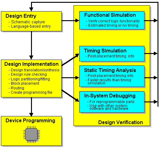
- Design Implementation
After the design is entered using schematic capture or synthesized, it is ready for implementation on the target device. The first step involves converting the design into the format supported internally by the tools. Most implementation tools read "standard" netlist formats and the translation process is usually automatic.
Once translated, the tools perform a design rule check and optimization on the incoming netlist. Then the software partitions the designs into the logic blocks available on the device. Partitioning is an important step for both FPGAs and CPLDs. Good partitioning results in higher routing completion and better performance for FPGAs and increased density and performance for CPLDs.
After the logic is partitioned into the logic blocks, the implementation software searches for the best location to place the logic block among all of the possibilities. The primary goal is to reduce the amount of routing resources required and to maximize system performance. This is a compute intensive operation for FPGAs and larger CPLDs. The implementation software monitors the routing length and routing track congestion while placing the blocks. In some systems, the implementation software also tracks the absolute path delays in order to meet user-specified timing constraints. Overall, the process mimics printed circuit board place and route.
When the placement and routing process is complete, the software creates the binary programming file used to configure the device.
In large or complex applications, the software may not be able to successfully place and route the design. Some packages allow the software to try different options or to run many iterations in an attempt to obtain a fully-routed design. Generally, try to use less than 85% of the available device resources. This technique provides the software extra resources to help route the design. Also, some vendors supply floorplanning tools to aid in physical layout. Layout is especially important for larger FPGAs because some tools have problems recognizing design structure. A good floorplanning tool allows the designer to convey this structure to the place and route software.
- Verification
Design verification occurs at various levels and steps throughout the design. There are a few fundamental types of verification as applied to programmable logic. Functional simulation is performed in conjunction with design entry, but before place and route, to verify correct logic functionality. Full timing simulation must wait until after the place and route step. After place and route, the software back-annotates the logic and routing delays to the netlist for simulation. While simulation is always recommended, programmable logic usually does not require exhaustive timing stimulation like gate arrays.
In a gate array, full timing simulation is important because the devices are mask-programmed and therefore not changeable. Plus a design change typically involves thousand of extra dollars in non-recurring engineering (NRE) costs and weeks of time. Compare this to a programmable device where changes are made in minutes to hours at little or no cost. In a gate array, you cannot afford to find a mistake at the silicon level.
One successful technique for programmable logic design is to functionally simulate the design to guarantee proper functionality, verify the timing using a static timing calculator, and then verify complete functionality by testing the design in the system.
Programmable logic devices have a distinct advantage over gate arrays. Changes are practically free. With in-system programmable (ISP) devices, such as SRAM-based FPGAs and ISP CPLDs, changes are possible even while the parts are mounted in the system. Using in-system verification techniques, the design is verified at full speed, with all of the other hardware and software. Creating timing simulation vectors to match these conditions would be extremely difficult and time consuming.
Some of the device vendors supply additional in-system debugging capabilities. For example, Xilinx ships a small pod called an XChecker cable that connects to your serial port and allows quick downloading of a design. With a few simple additions to your design and board, the XChecker cable is capable of stopping or single-stepping the clock and can read back the state of internal flip-flops. Likewise, Actel's Action Probes provide access to internal nodes within their anti-fuse based FPGAs.
One caveat�even though in-system debugging in quick and relatively easy, it should not be viewed as a complete replacement for simulation.
After creating a programming file, the programmable device is configured and ready for action. The actual programming method depends on the target technology. Most programmable logic technologies, including the PROMs for SRAM-based FPGAs, require some sort of a device programmer. For a nominal fee, your local distributor may do the actual production programming but a low-volume device programmer is generally required in the lab.
In-system programmable devices, including SRAM-based FPGAs, may not require a physical programmer but do require some intelligent system resource to download the programming file into the device. This is performed with a microprocessor, micro-controller, or via a JTAG test port.
Which companies supply programmable logic?
Ranked by 1997 sales volume (the last year that market data was available), the major high-density programmable logic suppliers are:
- Altera
- Xilinx
- Vantis (formerly AMD's programmable logic division, now part of Lattice)
- Lattice Semiconductor
- Actel
- Lucent Technologies
- Cypress Semiconductor
- Atmel
- QuickLogic
Other suppliers and additional vendor data is available on The Programmable Logic Jump Station.
The vendor summary table indicates which vendor supplies which architecture using which process technology.
I would like to try programmable logic but I don't want to spend a lot of money just yet. Where can I get inexpensive design tools?There is a list of free or low-cost software for programmable logic design, including schematic capture and synthesis tools available on The Programmable Logic Jump Station at
www.optimagic.com/lowcost.shtml
Different devices use different process technologies to build the memory cells used to program a device. Which one is best?Static Memory Technology (SRAM)
Similar to the technology used in static RAM devices but with a few modifications. The RAM cells in a memory device are designed for fastest possible read/write performance. The RAM cells in a programmable device are usually designed for stability instead of read/write performance. Consequently, RAM cells in a programmable device have a low-impedance connect to VCC and ground to provide maximum stability over voltage fluctuations.
Because static memory is volatile (i.e.-the contents disappear when the power is turned off), SRAM-based devices are "booted" after power-on. This makes them in-system programmable and re-programmable, even in real-time. As a result, SRAM-based FPGAs are common in reconfigurable computing applications where the device's function is dynamically changed.
The configuration process typically requires only a few hundred milliseconds at most. Most SRAM-based devices can boot themselves automatically at power-on much like a microprocessor. Furthermore, most SRAM-based devices are designed to work with either standard byte-wide PROMs or with sequential-access serial PROMs.
SRAM cells are also used in many non-volatile CPLDs to hold some configuration bits to reduce internal capacitive loading.
Vendors using SRAM technology: Xilinx FPGAs, Altera FPGAs, Actel (SPGA), Lucent FPGAs, Motorola FPGAs, DynaChip FPGAs.
Fuse
Fuse technology was the original programming technology for programmable logic. It is still used to manufacture bipolar SPLDs. A fuse is a metal link (connection) that can be programmed (open connection) by passing a current through the fusible link. Fuse technology is one-time programmable (OTP).Vendors using fuse technology: Texas Instruments
Anti-fuse
Anti-fuse is similar to fuse technology in that is one-time programmable (OTP). The anti- part of anti-fuse comes from its programming method. Instead of breaking a metal connection by passing current through it, a link is grown to make a connection. Anti-fuses are either amorphous silicon and metal-to-metal connections. They are usually physically quite small and have low on-resistance. Consequently, anti-fuse technology has benefits for creating programmable interconnect. However, they require large programming transistors on the device.Vendors using anti-fuse technology: Actel FPGAs, QuickLogic FPGAs
EPROM
Electrically Programmable Read-Only Memory. Similar to the technology used in standard EPROM memory devices. Commonly used in both SPLD and CPLD devices. EPROM cells are electrically programmed in a device programmer. Some EPROM-based devices are erasable using ultra-violet (UV) light if they are in a windowed package. However, most EPROM-based SPLD/CPLDs are in low-cost plastic packaging for production. Plastic packages cannot be UV erased.Vendors using EPROM technology: Xilinx, Altera, AMD, Cypress, Philips, Atmel, ICT, Waferscale Integration (WSI).
EEPROM (E2PROM)
Electrically-Erasable Programmable Read-Only Memory. An EEPROM memory cell is physically larger than an EPROM cell but offers the advantage of being erased electrically--no special UV erasers require. Plus, EEPROM devices can be erased, even in low-cost plastic packaging.FLASH
FLASH-erased (or bulk erased) electrically-erasable programmable read-only memory. FLASH has the electrically-erasable benefits of EEPROM but the small, economical cell size of EPROM technology.
Macrocell
A macrocell on most modern CPLDs contains a sum-of-products combinatorial logic function and an optional flip-flop. The combinatorial logic function typically supports four to sixteen product terms with wide fan-in. In other words, a macrocell may have many inputs, but the complexity of the logic function is limited. Contrast this to most FPGA logic blocks where the complexity is unlimited, but the logic function has just four inputs.
One-Time Programmable (OTP)
A one-time programmable device can only be programmed once. Once programmed, it cannot be re-programmed. All fuse- and anti-fuse-based devices are one-time programmable. EPROM-based devices in plastic packages are one-time programmable.
What does 'in-circuit programmable' or 'in-system programmable (ISP)' mean?
Though definitions vary slightly, in-circuit programmable or in-system programmable (ISP) means that the device can be programmed while it is mounted on the circuit board with the other components.Most ISP devices are built using SRAM, EEPROM, or FLASH technologies. All SRAM-based devices are inherently in-system programmable because they must be configured on power-up.
EEPROM and FLASH processes are erasable technologies. However, not all EEPROM- and FLASH-based are programmable while soldered on the circuit board. In-system programmability (ISP) requires special on-chip programming logic. Not all CPLDs have this logic, even if they are built with EEPROM and FLASH. Those lacking the on-chip programming circuitry are programmed and erased in a device programmer. Those with the programming circuitry either use a vendor proprietary interface or a JTAG (IEEE 1149.1) standard interface to re-program the device.
What general advice can you give to a programmable logic user?
- Buyer beware!
There is a lot of marketing hype out there from the suppliers about how fast, how big, and how inexpensive their devices are. Take all vendor claims with a grain of salt, especially when they talk about their competition. Programmable logic is wonderful stuff and it will match up with vendor's claims in a few years.
- Keep it synchronous.
Avoid gated clocks! Let me state that again: Avoid gated clocks! If possible, use a single clock for your entire design.
- Spaghetti code results in spaghetti logic.
Watch your VHDL or Verilog coding style (and that goes for CuPL, ABEL, AHDL, and the rest). The way that you describe your logic has a direct impact on how well or poorly the logic synthesizer can create your design. Good coding can produce designs that run twice as fast or consume four times less logic! Some of the logic optimization software out there is truly amazing, but they don't work miracles on a sloppy design.
- Keep it under 85.
Try to keep your logic utilization at 85% of the available resources or below. This makes it easier to place-and-route the design and allows sufficient room for future design iterations.
- Outsource.
Don't have time to learn how to use programmable logic? No problem. There are a number of highly-qualified design consultants and macro suppliers that can do miracles with programmable logic (I've seen some of their work). Don't be afraid to use them. Also, remember that most electronics distributors and vendors have their own design centers.
- Many devices are output disabled.
Most CPLD devices and some FPGA devices have just a few output-enable signals. Check the number of output-enable and open-drain outputs required by your design before you choose a device!
- CMOS does not mean low power.
In the old days, CMOS equalled low power. My, how things have changed. CMOS has very, very low static current. If your design just sits there, clocking at a few megahertz, power consumption is not an issue (well, unless you're using a CPLD, which has a much higher quiescent current--but that's another story). The faster you clock a CMOS device, the more power it consumes.
Therein lies the problem for modern system design. You almost always need more performance. So if CMOS burns more power the faster you go, what can you do to avoid melting the device? The easy way out comes to us via physics. CMOS power consumption is directly related to capacitance and the voltage, squared. Lower the voltage and voilà, down comes the power. How can you easily lower the voltage? Move to 3.3 volts or below. Many vendors now supply low-voltage devices.
- A little knowledge doubles your performance and your density.
Learn the underlying device architecture and you will be amazed at what you can achieve in programmable logic!
Where can I go for more information?The FPGA Site at
http://www.fpga-site.comprovides links to various device and development tool vendors plus connections to interesting research groups, books on programmable logic, on-line news groups, and various search engines and resources to find more information.
Copyright © 1997-2005 by OptiMagic™, Inc. All rights reserved.
All trademarks are the property of their respective owners.