|
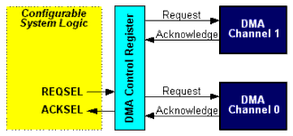
- DMA transactions are available from the Configurable System
Logic (CSL) matrix
- DMA Control registers
-- a special mode of an address selector
-- steer DMA requests and acknowledge signals to the appropriate DMA
channel
|
|
|
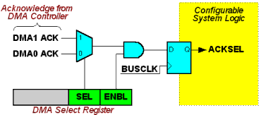
DMA Control Register
A DMA Control register has two control bits, duplicated in both the high and low nibble in the
byte-wide register.
|
7
|
6
|
5
|
4
|
3
|
2
|
1
|
0
|
|
-
|
-
|
SEL
|
ENBL
|
-
|
-
|
SEL
|
ENBL
|
- SEL steers the request/acknowledge signals
to and from the desired DMA channel.
- 0 = DMA Channel 0
- 1 = DMA Channel 1
- ENBL enables the particular DMA Control register. The
control register must be enabled before request/acknowledge signals are allowed to propagate
to the appropriate DMA channel. Ideally, only one DMA Control register should be enabled for
a particular DMA channel at any particular time.
The address of a DMA Control register is assigned similar to other address selector functions, by
assigning a symbolic address name.
FastChip Function Name: DMA Control Register
Schematic Symbol Name: DMACTRL
|
|
|
DMA Request Steering
- A Configurable System Logic (CSL) peripheral requests a DMA transfer by asserting
the REQSEL input on its associated DMA Control register.
- If the DMA Control register's enable bit, ENBL, is set,
then the request is forwarded to the DMA channel defined by the SEL bit.
If ENBL=0, then the request is ignored.
|

|
|
|
DMA Acknowledge Steering
- After a valid request, a particular DMA channel acknowledges the transfer.
- The requesting CSL peripheral receives the acknowledge via the ACKSEL
output on its associated DMA Control register.
|
|
|
|
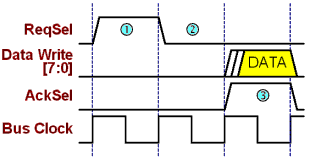
Example DMA Transaction from CSL Peripheral
Assume that a particular DMA channel is configured to perform a DMA Write operation.
- The CSL Peripheral asserts the REQSEL input on its
associated DMA Control register.
- The appropriate DMA channel recognizes the request.
- The DMA channel then presents the write data on the
CSI Socket's DATA WRITE bus. The CSL peripheral uses
the ACKSEL signal from the DMA Control register to latch the
data.
|
|